 مسكن
>
germanium transistor defect
مسكن
>
germanium transistor defect
منتج
أكثر من 30 نوعًا من المنتجات تغطي التعدين وسحق البناء والطحن الصناعي ومواد البناء الخضراء وغيرها من المجالات


germanium transistor defect
Trivalent Atom Defect-Complex Induced Defect Levels
5 之 Defect complexes have a significant impact on the structural, electronic, optical and electrical properties of semiconductors. Several defect complexes formed by n-type and p-type atoms in Ge have been
获取价格
Academic and industry research progress in germanium nanodevices
2011年11月16日 The extremely high number of defects formed in such a thin germanium layer would considerably degrade carrier mobility and augment junction leakage,
获取价格
Impact of Defects on the Performance of High-Mobility
2018年1月1日 An electrically active defect in a semiconductor generally gives rise to one or several localized energy levels in the bandgap, as illustrated in Fig. 5.2.This energy level
获取价格
Defect delineation and characterization in SiGe, Ge and other ...
2009年8月1日 Germanium is one of the most promising channel materials for complementary metal–oxide–semiconductor field-effect transistors (CMOSFETs), in
获取价格
Point Defect Engineering in Germanium - Massachusetts
In 1947, the first transistor was made of germanium, but soon silicon became the core material of computer chips because of its processability. However, as the typical
获取价格
Defects in Germanium - Photonics and Electronics with
This chapter discusses the atomoc and electronic structure of dopant impurities, point defects, Dangling Bond (DB), and hydrogen in germanium, along the way comparing
获取价格
Shaping the role of germanium vacancies in germanium telluride
2020年10月2日 Germanium telluride (GeTe) is a promising thermoelectric compound that contains a high number of missing-atom defects, or vacancies, within its crystal lattice.
获取价格
Thermodynamic Formation Properties of Point Defects in
Cowern and coworkers found that the point defects in silicon and germanium crystal transform from “point like” to “extended defects” as the temperature increases. The
获取价格
Germanium transistors : Sonic properties - Guitar Poppa
2015年6月21日 NOS germanium transistors, technology and tone properties : moderate gain, rounded knee, limited gain x bandwith product, leakage currents, beyond fashion. ... In all domains of audio, germanium transistors and their “good defects” are opposed to the cold pharmaceutical perfection of integrated circuits.
获取价格
Understanding mechanical properties and failure mechanism of germanium
2020年10月17日 Silicon-germanium (Si x Ge 1-x) is an alloy with any molar ratio of silicon (Si) and germanium (Ge).Si x Ge 1-x is a semiconducting and thermoelectric material that has been successfully deployed in heterojunction bipolar transistor, strained metal-oxide-semiconductor (MOS), complementary metal-oxide-semiconductor (CMOS), and many
获取价格
History of the transistor - Wikipedia
A transistor is a semiconductor device with at least three terminals for connection to an electric circuit.In the common case, the third terminal controls the flow of current between the other two terminals. This can be used for amplification, as in the case of a radio receiver, or for rapid switching, as in the case of digital circuits.The transistor replaced the vacuum
获取价格
The germanium quantum information route Nature Reviews
2020年12月21日 Vigneau, F. et al. Germanium quantum-well Josephson field-effect transistors and interferometers. Nano Lett. 19 , 1023–1027 (2019). Article CAS Google Scholar
获取价格
Doping (semiconductor) - Wikipedia
Doping of a pure silicon array. Silicon based intrinsic semiconductor becomes extrinsic when impurities such as Boron and Antimony are introduced.. In semiconductor production, doping is the intentional introduction of impurities into an intrinsic (undoped) semiconductor for the purpose of modulating its electrical, optical and structural properties. The doped material
获取价格Strain effects on polycrystalline germanium thin films
2021年4月15日 Accumulation-mode p-channel transistors based on the p-type Ge exhibited field-effect mobilities (170 cm 2 V −1 s −1) higher than those of most p-channel Si transistors 21.
获取价格
Sige Layers Defect of 28nm Node PMOSFETS In Advanced CMOS
Embedded SiGe as locally strained Si technology has been used to improve pMOSFET device performance through hole mobility enhancement. Embedded SiGe is achieved by selectively growing epitaxial SiGe film in recessed Si pMOSFET source and drain areas. However, selective epitaxy of SiGe will be increasingly challenging as germanium
获取价格
Germanium Based Field-Effect Transistors: Challenges and
2014年3月19日 Abstract. The performance of strained silicon (Si) as the channel material for today’s metal-oxide-semiconductor field-effect transistors may be reaching a plateau. New channel materials with high carrier mobility are being investigated as alternatives and have the potential to unlock an era of ultra-low-power and high-speed microelectronic ...
获取价格
Germanium transistors : Black Glass models - Guitar Poppa
2015年6月15日 Their leakage current, the generic defect of germanium transistors, is a bit higher than in later models. Forty years later I found them generally quite musical: Almost all of them combine a sonic color and a texture that makes them exploitable in preamps or boosters, overdrives and especially in fuzzboxes.
获取价格
Transistor - Wikipedia
The prefix is followed by a two-, three- or four-digit number with no significance as to device properties, although early devices with low numbers tend to be germanium devices. For example, 2N3055 is a silicon n–p–n power transistor, 2N1301 is a p–n–p germanium switching transistor. A letter suffix, such as "A", is sometimes used to ...
获取价格Why silicon and germanium are semiconductors - Test and
2016年2月9日 Silicon-germanium serves as a semiconductor in integrated circuits for heterojunction bipolar transistors or as a strain-inducing layer for CMOS transistors. Here heterojunction refers to the interface between two layers or regions of dissimilar crystalline semiconductors. The two semiconducting materials have unequal band gaps.
获取价格
Monolayer black phosphorus and germanium arsenide transistors
2023年12月4日 Two-dimensional (2D) semiconductors could be used as atomically thin channels in future transistors, providing immunity to short-channel effects 1,2,3,4.In conventional bulk semiconductors ...
获取价格
Growth and Selective Etch of Phosphorus-Doped Silicon/Silicon–Germanium
2020年12月9日 Growth and Selective Etch of Phosphorus-Doped Silicon/Silicon–Germanium Multilayers Structures for Vertical Transistors Application. ... The indicator for the defect density in HRRLMs is the broadening of SiGe layer along ω-direction (ω is the incident beam angle). ... This work was funded by “Research on Novel
获取价格
Shaping the role of germanium vacancies in germanium telluride
2020年10月2日 Understanding and controlling point defects in semiconductors are essential for developing advanced electronic and optoelectronic devices. Germanium telluride (GeTe), a semiconductor with a ...
获取价格
Why silicon and germanium are semiconductors - Test and
2016年2月9日 Silicon-germanium serves as a semiconductor in integrated circuits for heterojunction bipolar transistors or as a strain-inducing layer for CMOS transistors. Here heterojunction refers to the interface between two layers or regions of dissimilar crystalline semiconductors. The two semiconducting materials have unequal band gaps.
获取价格
Monolayer black phosphorus and germanium arsenide transistors
2023年12月4日 Two-dimensional (2D) semiconductors could be used as atomically thin channels in future transistors, providing immunity to short-channel effects 1,2,3,4.In conventional bulk semiconductors ...
获取价格
Growth and Selective Etch of Phosphorus-Doped Silicon/Silicon–Germanium
2020年12月9日 Growth and Selective Etch of Phosphorus-Doped Silicon/Silicon–Germanium Multilayers Structures for Vertical Transistors Application. ... The indicator for the defect density in HRRLMs is the broadening of SiGe layer along ω-direction (ω is the incident beam angle). ... This work was funded by “Research on Novel
获取价格
Shaping the role of germanium vacancies in germanium telluride
2020年10月2日 Understanding and controlling point defects in semiconductors are essential for developing advanced electronic and optoelectronic devices. Germanium telluride (GeTe), a semiconductor with a ...
获取价格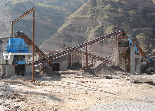
Trivalent Atom Defect-Complex Induced Defect Levels in Germanium
5 之 Defect complexes have a significant impact on the structural, electronic, optical and electrical properties of semiconductors. Several defect complexes formed by n-type and p-type atoms in Ge have been implemented for the development of improved modern microelectronic devices. However, there is no reported study on the substitutional
获取价格
Full article: Germanium epitaxy on silicon - Taylor Francis Online
2014年3月18日 Introduction. The first transistor was created in 1947, using germanium bulk crystals as raw materials. Germanium has a lot of advantages over silicon, among which the larger hole and electron injection velocity and mobility can provide the semiconductor devices with higher frequency operation. But due to the lack of stable
获取价格
Bipolar junction transistor - Wikipedia
The germanium transistor was more common in the 1950s and 1960s but has a greater tendency to exhibit thermal runaway. Since germanium p-n junctions have a lower forward bias than silicon, ... Radiation causes a buildup of 'defects' in the base region that act as recombination centers. The resulting reduction in minority carrier lifetime causes ...
获取价格
Growth, structural, and electrical properties of germanium-
2017年9月18日 In order to address the challenges of developing Ge devices on Si substrates, this paper investigates the viability of direct Ge-on-Si heteroepitaxy via solid source molecular beam epitaxy (MBE).By studying the carrier transport properties, oxide-semiconductor heterointerface characteristics, and structural defects inherent to the as
获取价格The Lost History of the Transistor - IEEE Spectrum
2004年4月30日 In early 1952, after much wheedling and cajoling by Haggerty, TI purchased a patent license to produce transistors from Western Electric Co., ATT’s manufacturing arm, for $25 000. By the end of ...
获取价格
Seventy-Five Years since the Point-Contact Transistor:
2022年11月24日 offered for reviewing Germanium in the spirit of recalling its original role at the onset of the semiconductor revolution 75 years ago and its great promise for the future. In the present review we considered (a) transistors and artificial intelligence and (b) the key Ge defect-engineering processes and their impact on devices and (c) highlighted
获取价格
IEEE TRANSACTIONS ON ELECTRON DEVICES, VOL. 63, NO. 8,
A tech-nology computer-aided design model of extended defects is developed based upon measured device electrical properties. single extended defect is introduced into simulated 2-D planar and 3-D FinFET structures. It is found that a 2-D extended defect is a source of variability in planar transistors, with the electrical effects depending on ...
获取价格
Impacts of oxygen passivation on poly-crystalline germanium
2014年4月30日 The leakage in a poly-crystalline germanium (poly-Ge) transistor was well suppressed. It is indicated that the residual oxygen can passivate the defects in poly-Ge. We investigated the effects of the annealing ambient during solid phase crystallization (SPC) on the crystallization temperature of amorphous Ge and the electrical properties of a ...
获取价格
power supply - Why did my transistor break? - Electrical
2020年9月4日 The original delayed fuse of 10A has been replaced by an INSTANT FUSE OF 10A. This because the delayed fuse has burnt only after some seconds, and that time has been enough to break the transistor. A REVERSE DIODE has been put in parallel to Base-Emitter Junction of the BUV20. A ZENER DIODE OF 24V, 5W has been put in
获取价格
Silicon-Germanium Bipolar Technology SpringerLink
2012年1月1日 In chapter 3 the silicon-germanium technology used throughout this work is presented. First, different large-signal models and operating points of a bipolar transistor are explained. Additionally, a small-signal model in the active forward region with the resulting small-signal parameters is introduced. The influence of parasitic elements on ...
获取价格